
A brief story of the project start with the excelent ADX Transceiver from Barb (WB2CBA) which can be found at
The ADX transceiver is powered by an Arduino Nano (ADX) or Arduino Uno (ADX_UNO) boards using both the ATMEL ATMEGA382p processor.
In order to leverage the capabilities of the transceiver with a powerful processor such as the Raspberry Pi Pico which uses the rp2040 architecture a project called ADX-rp2040 was started.
Then a map between the Arduino board I/O and the rp2040 I/O was made showing some differences needs to be addressed which requires additional circuitry.
As an evolution of that project the goal to reduce the footprint of the transceiver, trying to remove the signal generator function (Si5351 based), this effort leads to this project.
The project aims to achiveve several (experimental) goals:
- Port the ADX firmware to the rp2040 (already done with the ADX-rp2040
- Design and develop a hardware board to support the project
- Implement a USB digital audio interface, the board can be seen as a virtual sound card.
- Implement an all Raspberry Pico based DDS generation (no Si5351 board).
Once implemented an ADX class FT8 digital transceiver can be created using different hardware strategies.
Basic specs for this transceiver would be:
- Operate in any of the HF bands (160m to 10m), attempts to marginal use on 6m will be made.
- 2-3W output (WSPR,FT8;JS8,FT4).
- Different alternatives for receiver:
- DC (CD2003GP).
- Ssuperhet (CD20023GP)
- Digital (Si4732 based)
- SWR protection.
- Beacon mode (WSPR,FT8).
- ATU reset output.
- PA SWR protection (zener diode).
This project relies heavily on the superb work made by several authors:
-
Roman (R2BDT) with his pico-WSPR-tx project (link) which in turns relies on his pico-hf-oscillator project link
-
Hitoshi-san (JE1RAV) with his QP-7C_RP2040 project did most of the heavy lifting to use a USB for both digital audio and serial interface (CDC). link.
-
As said the ADX architecture has been originally developed and promoted by Barb (WB2CBA) and had been spinned off by dozens of experimental implementations, most of the transceiver hardware is rooted on his signature original design.
-
The ADX-rp2040 firmware was originally developed by me as an adaptation of the ADX Arduino firmware, differences with the original code were quite large so the actual final code was refactored in the process. link
-
An early effort called RDX-rp2040 was originally developed as a stand alone FT8 transceiver able to operate without a PC, the project reach the prototype stage and stays there since. Part of the hardware and the si4732 utilization comes out of it, not being an optimal implementation the board designed for that project can also be reused. link
-
Hans Summers (G0UPL) developed the original QCX transceiver, which creates a whole family of high performance, yet affordable, homebrew transceivers.
-
Guido (PE1NNZ) who developed the original uSDX microcode for the Arduino which inspired manyfold designs, specially the uSDX class transceivers, and opened the gate for a generation of low cost at reasonable performance ham radio equipment.
With enough luck and cooperation this project might turn into a system which includes the different components in order to be reproduced, lots of work needs to occur for this to happen.
73 de Pedro (LU7DZ/LT7D)
This is an experimental, work-in-progress, non-profit project performed as closest to the ham spirit as possible. Only spare, hobby, time is available to move the project forward or to provide support on usage or issues.
Until further notice is provided this project is work in progress and not able to be reproduced directly.
If anybody has questions or issues please:
- Be sure you read the documentation first.
- Check on the issues list of the GitHub site, the issue might have been described there or even a workaround might exists for it.
- State it as an English request. English isn’t even my fourth language, still I do my best to adhere to it.
- For casual question you can use the groups.io uSDX forum and for a longer ones please open and issue at the GitHub portal of the project.
- Express very clearly which version and level the firmware has. In most cases using the latest would solve the issue.
- Ensure the issue happens with a freshly downloaded last version of the firmware, don’t expect me to debug any modification you did.
- Describe in your own words the problem and what you did to expose it and what workarounds you attempted.
- Add the content of the monitoring terminal session with DEBUG enabled to help me understand what is going on.
- Attach any other documentation you think might help debugging the issue.
Please report ONE (1) issue per entry, and proceed as clean as possible with the debug instructions given to you to further understand or to fix the problem. I’ll address your issue as soon as my available time allows, not necessarily in a FIFO way.
The overall program architecture can be seen in the following activity graph

The main Transmit-Receive cycle loop can be seen in the following activity graph

This is the first version of the firmware, the main functions implemented are:
- Operate in any of the HF bands (160m to 10m), attempts to marginal use on 6m will be made.
- 1W RF power, DC receiver (CD2003GP based) with SWR protection.
- Management of the ADX-ddsPIO board.
- Receive and transmit digital audio data over a USB connection.
- Is able to operate with weak mode signals.
The firmware is completed at this stage and able to sustain QSO as shown in the following picture
where a contact is been made between the board (dubbed as LU2EIC) and my 20m digital FT8 station
running as LU7DZ using a direct conversion receiver setup.
 Although the RF setup is close to trivial, just few meters distance, the activity has been held
"over the air" and shows the firmware is able to properly encode and decode signals both at the
audio and RF levels. My 20m station is composed of a QDX transceiver being run by a Raspberry Pi
controller running a modified version of WSJT-Z whilst the testbed for the ADX-ddsPIO is my
Mac running the MacOS version of WSJTX. For all practical purposes this is considered the
"maiden QSO" of the board and all goals for this level can be called as completed.
Features
- Permanent settings (EEPROM emulation).
- CAT control (TS2000 emulation).
- Superhet ADX-S support.
- Implementation of a BFO (465 KHz) local oscillator.
- Quadrature based receiver (SDR) support (quadrature clock available)
- Si4732 based receiver chipset support
- USB (MSC) drive filesystem implementation to store external configuration (CONFIG.SYS)
The firmware is completed at this stage and able to sustain QSO as shown in the following picture
where a contact is been made between the board (dubbed as LU2EIC) and my 20m digital FT8 station
running as LU7DZ using the Si4732 chip as a receiver.

The development environment used is Visual Studio code using the standard Raspberry Pi Pico C/C++ SDK.
Please follow the official documentation of both to install and configure the functionality.
The firmware could be flashed directly to the Raspberry Pi Pico (rp2040) processor on the board following the conventional BOOTSEL method.
The file to flash is ./src/build/ADX-ddsPIO.uf2 .
I started the porting of the firmware assuming an ADX transceiver board, no more but no less features, but being powered by a Raspberry Pico board; the porting of the software was a great deal of a learning curve not only for the rp2040 architecture being different from the ATMEGA382p and being more powerful, but also a substantially different build chain which in some cases is implementing partially some features. For migration purposed the Raspberry Pi Pico board was used.
At his point the Raspberry Pi Pico (standard) and the RP2040 Zero boards are supported.
The Raspberry Pi Pico W (wireless) is not supported.
This circuit is largely based on the former RDX_rp2040 project design and it's compatible
with that board design with just minor mods.

The main differences with the verion 1.x:
- The receiver configuration has been changed to use the Si4732 receiver chipset.
A new, fresh, board design will eventually be made, however the development is supported with a prototype based on a modified RDX_rp2040 board.
Modifications could be made to the RDX board to operate with firmware level 2.x or up main advantage at this point is the availability of a PCB design which allows the usage of SMD components easily.
The required mods for the RDX board to work with the ADX-ddsPIO firmware are:
- Cut the PCB wire PICO ADC0 (GPIO26) to R10/R11/C10.
- Run a wire from R10/R11/C10 to PICO ADC2 (GPIO28).
- Run 2 pullup 10K resistors from PICO GPIO16 to +3.3V and GPIO17 to +3.3V.
- Do not use a Si5351 breakout board
- Run a wire from GPIO13 to the CLK0 pin of the Si5351 place.
- Run a 10K pullup resistor from Si4732 pin 3 (INTB) to +3.3V.
- If running with an external +12V cc supply remove jumper J7.
Work in progress
This circuit is largely based on the ADX transceiver modification made by Hitoshi Kawaji (JE1RAV) and
marketed as a kit form by Adam Rong (BD6CR) at CRKits.com (link ).

The main differences with the verion 0.x:
- The receiver configuration has been changed to a superhet.
This circuit is largely based on the original ADX transceiver link by Barb (WB2CBA)
modified for the rp2040 processor at the ADX-rp2040 project.

The main differences with the original ADX circuit are:
- Si5351 module no longer present.
- Analog audio circuit has been removed as the audio information is received digitally thru USB.
The pinout assignment for this version is shown in the following table:

A simple FAT-16 (MS-DOS) filesystem is implemented using a USB (MSC) interface, although the space is very limited it can be used to store any file on it. When plugged the name of the inserted device will be ADXDISK.
The firmware uses just one of them called CONFIG.SYS which stores a master configuration for the board, if the board is initiated with the file system empty (first boot) a CONFIG.SYS file with the default configuration will be written. In order to reset the board content (and the flash memory containing the configuration) the power up needs to be made while keep pressing the TX switch (the default LED will flash quickly), upon release the file content will be erased and the CONFIG.SYS file regenerated with the default configuration values.
This is a sample of a CONFIG.SYS file managed by the system
{
"ID" : 1,
"mode" : 4,
"slot" : 3,
"volume" : 60,
"bandwidth" : 1,
"frqFT8" : 14074000
"frqbfo" : 446400
}
Because of it's simplicity the filesystem will not support directories.
The logic is as follows:
- The main default configuration (sort of a factory default) is stored as constants defined at build time.
- If EEPROM is enabled
- the factory defaults are stored in EEPROM to make them persistent.
- If FS is enabled
- will override the EEPROM directive and take configuration from the CONFIG.SYS file.
- If the CONFIG.SYS file is erased the next boot the default configuration will be taken and a new CONFIG.SYS file created.
- Any change in the CONFIG.SYS file will be made permanent by properly EJECT the USB device in the host computer.
- Either the content of the EEPROM or the FS will override the factory defaults.
Both methods are sort of redundant and will not operate at the same time, whether the configuration is stored in EEPROM, File system or not stored is configured at build tiime by means of the configuration options choosen.
- (not EEPROM && not FS) the configuration will not be persistent across reboots, any change made during operation will be lost once the board is powered down.
- (EEPROM && not FS) the configuration will be persistent across reboots, it will start with the defaults but any change will be stored in EEPROM and recovered in the next boot.
- (not EEPROM && FS) the configuration will be taken from the CONFIG.SYS file and override the board defaults, however any change made won't be saved into the CONFIG.SYS file and therefore will be lost when the board is powered down. However, changes made externally on the CONFIG.SYS file will be taken on the next boot and on. All changes made externally on the CONFIG.SYS file will require the media to be ejected to become permanent.
- (EEPROM && FS) if this configuration is detected FS will be taken and EEPROM discarded at bootup.
The board defaults can be changed and made effective by changing the configuration options and recompiling the firmware.
- (not EEPROM && not FS) no configuration to clean up, powering down and up the board will restore the defaults.
- (EEPROM and not FS) powering up the board with the TX switch pressed will reset the EEPROM to the board defaults.
- (FS and not EEPROM) erasing the CONFIG.SYS file (or editing it) and ejecting the USB media will clean up the configuration.
- (FS and EEPROM) FS will prevail.
The configuration at build time is set by a number of #define clauses
#define  DEBUG      1     //Will enable the traces to be sent thru Serial Monitor, also the boot will stop until it is enabled
#define  EEPROM     1     //Enable EEPROM simulation in flash memory
#define  SUPERHET   1     //Enable the creation of a 455 KHz BFO signal
#define  QUAD       1     //Enable the creation of a Quadrature oscilator signal (SDR operation)
#define  SI4732     1     //Enable the support for the Si4732 chip
#define  WAITSERIAL 1     //Enable waiting for the Serial Monitor to be up to continue loading
#define  FS         1     //Enable file system FAT-16
#define  RTC        1     //Enable real time clock and time sync (partially implemented)
#define  CAT        1     //Enable CAT support
Some of the features conflicts among them so there is a dependency filter setup as follows that should not be modified.
#ifdef FS                        //EEPROM emulation or USB file system, FS prevails
#undef EEPROM
#endif //FS

#ifdef SI4732                    //If Si4732 chipset enabled it's the dominant receiver
#undef SUPERHET
#undef QUAD
#undef RTC
#endif //SI4732

#ifdef CAT                      //If CAT enabled USB can not be used to debug
#undef DEBUG
#undef RTC
#endif //CAT

#ifdef QUAD                     //If Quadrature oscillator activated all other clocks disabled
#undef SUPERHET
#undef SI4732
#endif //QUAD

#ifndef DEBUG                   //If not in DEBUG mode will not wait for Serial Monitor to activate
#undef WAITSERIAL
#undef RTC
#endif //!DEBUG
The board supports and the firmware implements several clock models which can be configured for different board setups.
- Dual clock (DC Receiver).
- Dual clock + IF (Superheterodyne)
- Quadrature (SDR)
In this setup the clock is produced simultaneously from GPIO13 and GPIO14, both signals are identical, both in receiving or transmitting mode. It's intended to make the circuit simpler. Actual operation of the board will require other signals such as RXSW and TXA to properly operate to be controlled by the firmware. This clock also uses a derivative of the VCO done by Roman (R2BDT) modified to replicate the output of the PIO on pins GPIO13 and GPIO14 simultaneously.
Then the board operates with a superheterodyne receptor configuration the receiver process requires two clocks, the main one to operate the down-converter mixer from the HF frequency to an intermediate frequency and other as the intermediate frequency oscillator frequency.
The down-converter local oscillator (RFLO) can be either one of the clocks despicted above.
The intermediate frequency clock (RFIF) is a special clock, it's lower in frequency and therefore it's easier to implement on a processor with limited resources. Also it's a fixed frequency as it doesn't vary with the operation.
Unfortunately attempts to extend the VCO concept to simultaneously create a different clock at a different frequency prooved to be beyond the limits of the processor; the VCO uses for itself a whole core (core1) in blocking mode so no other task can be interleaved without causing jitter, spurious outputs or frequency drift or all three together. At the same time the other core (core0) it's actually devoted to provide all the other tasks of the board such as USB Audio, USB CDC (serial), board management, signaling, timers, etc.
A different approach is then intended. the rp2040 processor has several specialized processors called PIO (Programmable Input/Output) which are a limited memory, limited instruction set (RISC) processors but completely independent from the main processor. Each processor executes their program as part of a state machine (SM) which dictates which instruction is executed at each clock cycle. They are programmed in a special Assembler language (PioASM) and are extremely useful to perform I/O without tying up the processor or forcing the handling of interrupts on the main cores.
To generate a clock for the intermediate frquency a PIO is assigned with that purpose
the state machine (SM) of the selected PIO runs at the frequency
For an estimated 465 KHz frequency for the IF of the receiver then
The clock used by the PIO is derived from the system clock (
However, the actual divisor used by the rp2040 has a resolution of 1/256, so in this case:
where:
The ideal divisor would be
As the hardware allows only for steps of
A split is made:
A split needs to be made
And the real frequency obtained would be
The quantization introduces then an error of
Being the relative error
This error factor is accounting only for the fractional divisor error of the PIO. Other sources of error needs to be considered such as
- Board crystal tolerances.
- PLL error.
- Thermal drift.
- Fractional divider internal jitter.
However, the level of error obtained is a good compromise between performance, cost and simplicity.
The waveform obtained at GPIO15 is as follows for a nominal

The outputs at GPIO13 and GPIO14 would be a clock at the operating frequency whilst the output at GPIO15 (when option #define SUPERHET 1 is set) would be a fixed clock of the established frequency (normally in the 450 KHz range) as shown in the following picture.

This option is activated with the compilation directive #define SUPERHET 1
This option is deactivated with the compilation directive #define QUAD 1
If a Software Defined Radio (SDR) receiver is needed the board has to provide two specific signals
called by convention clock I and clock Q which are of the same frequency but whose phases are
90
Again, trying to obtain such signal using the VCO technology it's quite difficult with the resources available, an approach to create them using again a PIO processor with that purpose is made.
The result is a digital quadrature frequency synth (I/Q) and it's architecture and logic follows.
This option is activated with the compilation directive #define QUAD 1
This option is deactivated with the compilation directive #define SI4732 1
When the board uses a Si4732 based receiver the clock generated by the rp2040 is only needed for transmission as the receiver generates it's own clock.
For simplicity the transmission clock (CLK0 and CLK1) are turned off while in reception and turned on while on transmission.
This option is activated with the compilation directive #define SI4732 1
This option override all other configuration options
The architecture combines:
- Dynamic reconfiguration of the board clock (PLL_SYS).
- Generate quadrature signals using a 4-state PIO logic.
- Manipulate the fractional divisor (Q8.8) of the PIO state machine.
- Perform a frequency optimization of the error.
The system achieves typical errors in the 0-50 Hz range over the HF spectrum, being the receiver clock and being stable on that error this is quite compatible with digital modes such as FT8, the only effect would be than the "nominal" frequency of the incoming signal with be shifted up or down by the error (few Hz) in a stable way.
Main components are
- PLL_SYS (RP2040).
- Main boar clock (clk_sys).
- Configurable divider:
- refdiv
- fbdiv
- postdiv1
- postdiv2
- PIO (Programmable I/O)
The PIO executes a cyclic firmware with 4 states which generates the quadrature signal over 2 output pins
00 → 01 → 11 → 10 → repeat
Each instruction is executed in one clock cycle of the state machine, therefore manipulating the clock of that PIO state machine using a fractional divider the output frequency can be manipulated:
Selecting two consecutive pins the signals I and Q can be extracted from each.
The synthesis math model follows
Each instruction of the PIO is executed in:
In order to complete a full period all 4 instructions needs to be executed
Therefore the output frequency (
Using
Results
Which is the master equation of the system operation
When a target frequency (
But the hardware is limited to
Therefore not all values of
And the true frequency resulting would be
and the error
When computed over the HF range the error could become quite large, from several Hz in the lower bands to close to 30 KHz in the higher bands, this is not acceptable.
To minimize the error two factors needs to be defined, the divisor but also the system clock in a way that an exploration of the discrete space of solutions
$refdiv\in[1,16]$ $fbdiv\in[16,320]$ $postdiv1\in[1,7]$ $postdiv2\in[1,postdiv]$
With:
$f_{ref}=\frac{f_{xosc}}{refdiv}$ $f_{vco}=\frac{f_ref}{fbdiv}$ $f_{clk}=\frac{f_{vco}}{postdiv1 \times postdiv2}$
Subject to the following constraints:
$400 \text{MHz} \le f_{vco} \le 1600 \text{MHz}$ $f_{clk} \le f_{max_sys}$
A minimization optimization problem can then be solved with the following border conditions
For each valid PLL configuration a computation is made
All candidates are evaluated
For each
Searching for the minimum of
Selecting as a result the value with the minimum absolute
error
This is a discrete search with a double optimization:
- PLL quantization.
- Divider (Q8.8) quantization
The theoretical error limit is
taking derivatives
Being the approximate máximum error value:
Since
results $\left \lvert {\epsilon}{max} \right \rvert \approx \frac{f{req}^2}{2 \times f_{clk} \times 64}$
As a consequence
- Error is reduced when
$clk_{sys}$ increases. - Error grow quadratically with the
$f_{req}$ - The divisor cuantization controls the residual error.
A typical expected result would be
| Band | Freq | clk_sys | Error |
|---|---|---|---|
| 80 m | 3 573 000 | 167 428 571 | 0 Hz |
| 40 m | 7 074 000 | 233 000 000 | ±3 Hz |
| 20 m | 14 074 000 | 268 285 602 | ±2 Hz |
| 15 m | 21 074 000 | 178 800 000 | ±30 Hz |
| 10 m | 28 074 000 | 261 000 000 | ±50 Hz |
The output of this clock is implemented to be obtained at pins GPIO14 (I) and GPIO15 (Q).
The resulting waveform is similar to the following example (for 3.5 MHz)

This clock is activated by the directive #define QUAD 1
The following test resources has been built
In order to develop the first stages of the firmware a reduced mockup has been used
 This reduced scope board contains just the processor and the push buttons. A small
RF probe is feed into a wire for local "on the air" tests.
To continue developing the board a first cut prototype board is built as shown in the
figure
 The building technique is to make connection with hand made wiring, the Raspberry Pi Pico
board has been replaced with a rp2040 Zero board which is essentially the same but with
a much smaller footprint. The main disadvantage of this board is that not all the GPIO
pins are expossed, but still as the ADX-ddsPIO board uses just few GPIO lines it's quite
adequate.
Just the transmitting part sans finals has been made as yet as the measurements associated
with the firmware development requires large periods with the board in TX mode and there
is no point on running finals for that.
To continue the development of the firmware adding the reception sub-systems an extended
prototype including a receiver has been built.
 This prototype contains the processor, the RF driver and the simple CD2003GP based
DC receiver. The processor board used is the breakboard rp2040Z which provides the
same funcionality than the Raspberry Pi Pico with a reduced availability of GPIO and
other pins but with a much smaller board footprint.
A small RF probe is feed into a wire for local "on the air tests".
To continue the development of the firmware adding the Si4732 based receptor a modified version of a board from the RDX-rp2040 project has been used with small mods in order to adapt for the differences

Mods follows:
Work in progress
This utility is a reduced firmware implementing the DDS using a fixed frequency given by the GEN_FRQ_HZ parameter in the ddsTest.h file. It's main purpose is to explore the concept and the initial measurements using the Raspberry Pi Pico as an RF generator. Also to integrate the code originally on the pico-hf-oscillator package on this project.
This code is a crude porting of the test.c program from the pico-hf-oscillator package
This utility has been created as a reduced scope test bed for the board and some of the DDS functions applied to the generation of FT8 signals.
- When boot if the SYNC button IS KEPT pressed the firmware waits and upon release enters the FT8 test mode, it's important the SYNC button is released as close to the top of the minute (sec=0) of any minute. In this way the internal clock is set at a random date time but the second is synchronized. At the start of each minute a fixed message is sent using FT8. The message to be sent can be changed by modifying the message memory area, the base frequency (and band) can be set changing the GEN_FRQ_HZ (in Hz) parameter and the shift within the FT8 sub-band changing the FT8_BASE_HZ (in HZ) parameter. While activated in this mode the TX can be turned on by pressing the TX button.
The following figure shows how WSJT-X receives the local message

When using a wire out of the GPIO 18 pin to transmit "on the air" signals the spectrum
is *extremely* dirty. Do not put this signal into any meaningful antenna and use it
only by short evaluation tests.
This utility continues the integration of the firmware system incorporating the features of the ADX board such as UP/DOWN buttons, TX button and the four mode LED (FT8,FT4,JS8 and WSPR) as well as the TX LED. The board continuously generates an RF signal, when in RX mode (RXSW high) the output is connected with the receiver (RXOSC) whilst when in TX mode (RXSW low, TX high) the output is connected to the driver section. If properly synchronized (see testFT8) upon start the firmware sends a message at the top of every minute using the defined frequency and mode.
When using a wire out of the GPIO 18 pin to transmit "on the air" signals the spectrum
is *extremely* dirty. Do not put this signal into any meaningful antenna and use it
only by short evaluation tests.
This utility is a strip down version of QP-7C_rp2040_cat with both the USB audio and serial data enabled. The USB audio stream is read and the frequency computed averaging the results every 10 mSecs, the result is displayed thru the serial monitor (while the USB audio continue working) showing both the frequency counting algorithm and the operation of the USB serial monitor.
The test configuration needs the followigh steps:

* Compile and load the firmware.
* Open the serial monitor pointing to the */dev/tty.usbmodem00000xx - TinyUSB* device
* Start the supervision of the serial monitor channel.
* Start WSJTX and configure in the AUDIO tab
	* Input: ADX-ddsPIO
	* Output: ADX-ddsPIO
* Start the TX Tone, the serial monitor should mark the tone frequency as set in WSJTX.
* Start the FT8 TX, the serial monitor will show the different tones sent.


The counting algorithm has +/- 1  Hz accuracy, this can be improved later choosing
the averaging time, but should be enough to properly decode the frequency and
change it accordingly.
This is a hack to integrate the Audio USB version (testUSB2) with the DCO version (testADX) into a single firmware, crude at best, but mainly intended to explore and resolver the (really many) hardware conflicts and library incompatibilities.
For most part it's a functional transmitter as shown in the following picture where a local copy of WJST-X running on a Mac (test station) is evaluated in my main WSJT-X station, it can be seen the transmission and the decoding of it.

At the bottom of the image the WSJT-X configuration dialog can be seen where the input and output devices is actually the ADX-ddsPIO board recognized as such.
This is the prototype of the digital quadrature frequency synth (I/Q) clock
It's just used to evaluate the overall performance and yield unmodulated clock signals thru ports GPIO14 (I) and GPIO15 (Q)
This is the prototype and test bench for a rp2040 based si4732 library
This is the prototype and test bench for a configuration filesystem (FAT) to support a configuration file (CONFIG.TXT) using the board as a USB MSC (aka pen drive).
There are other implementations which aren't functional by itself but only part of prototype and experimentation efforts on specific aspects.
- testUSB Algorithm for frequency measurement over the USB audio channcel.
- QP-7C_rp2040_cat Full implementation of USB Serial and Audio.
Unless otherwise specified do not expect to flash these projects on a raspberry pi pico
and obtain any functionality
(Excerpts from the original package pico-hf-oscillator by Roman Piksaykin (R2BDY) https://www.qrz.com/db/R2BDY
The pico-hf-oscillator library for Raspberry Pi Pico includes the headers and source code and all necessary build files to build a custom application which turns pico into precise PLL digital frequency oscillator of the whole of HF radio spectrum (1 Hz to 32.333 MHz) with millihertz resolution.
The library provides about 23 milli-Hz frequency resolution. This resolution is limited by 24-bit register which is used in algorithm. A workingWSPR beacon which has been built on the base of this project proves that the quality of generated signal is sufficient to such precise (~1.46 Hz step) frequency manipulation digital modes.
The upper freq. limit is ~32.333 MHz and it is achieved only using Pico overclocking to 270MHz.
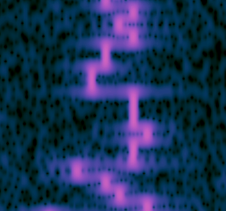
Here is an example of narrowband FSK (9.4 MHz carrier, 5 Hz step, 20 Hz range in total).
The DCO uses phase locked loop principle programmed in C.
The DCO provides the output signal on the GPIO pin. However if you want to transmit the signal, you should calculate and provide a lowpass filter of appropriate frequency. Please also figure out whether you possess rights to emit radio frequency energy on desired frequency.
GPS reference frequency correction option provides an absolute frequency error within about ~1Hz in long term.
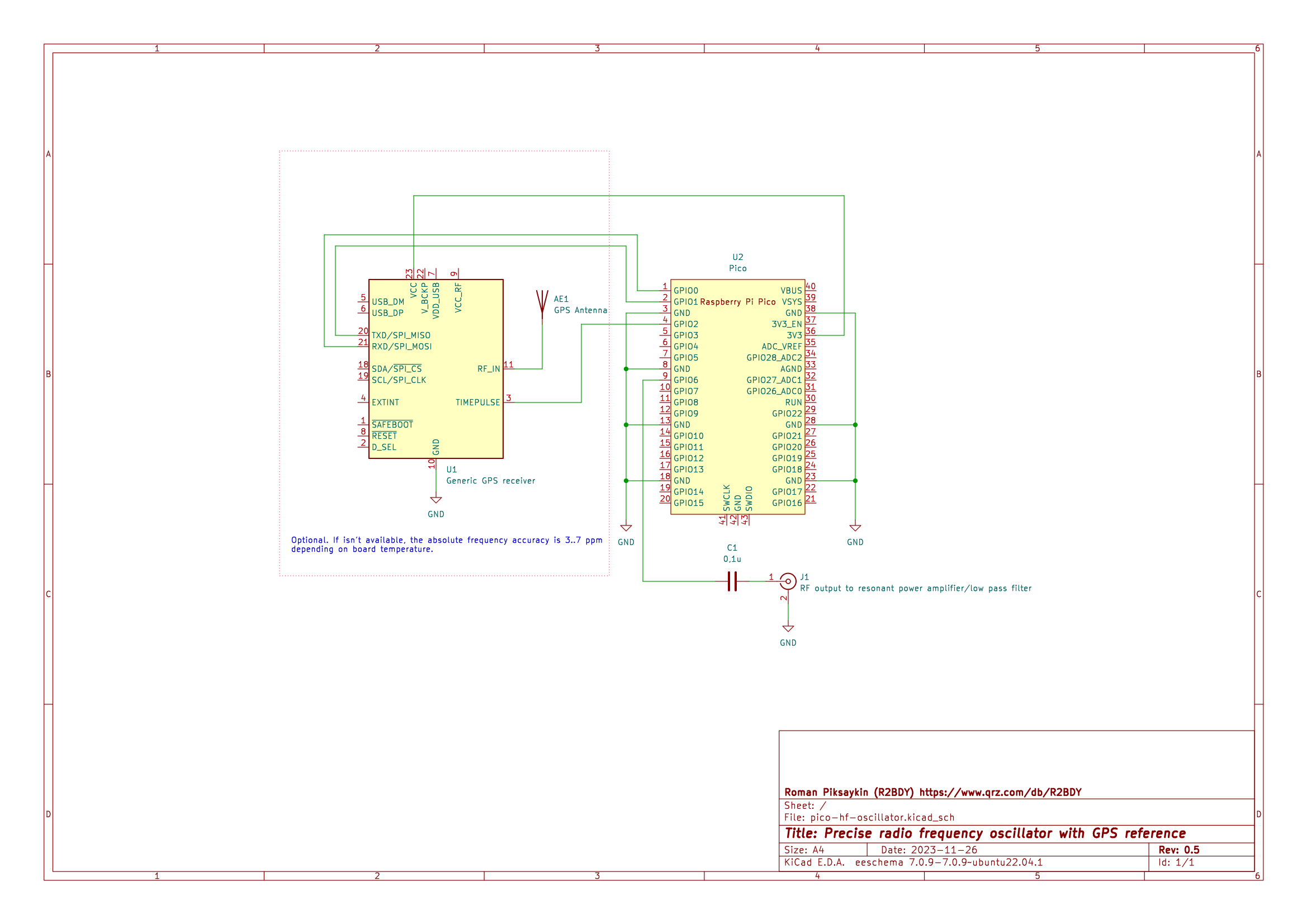
The DCO uses extensively the secodary core of the pico. The first one is for your ideas how to modulate the DCO to obtain a desired signal. The DCO does NOT use any floating point operations - all time-critical instructions run in 1 CPU cycle.
Owing to the meager frequency step, it is possible to use 3, 5, or 7th harmonics of generated frequency. The practical resolution will be quite the same - far below 1 Hz. Such solution completely cover all HF and VHF band up to ~233 MHz.
Roman will appreciate any thoughts or comments on that matter.
Roman Piksaykin, amateur callsign R2BDY https://www.qrz.com/db/R2BDY